Micro & Nanotechnologies
Micro & Nanotechnologies expertise and related facilities are available in PEIC through the CHILAB-ITEM (Interfacing Technologies for Edge Microsystems) belonging to the Department of Applied Science and Technology (DISAT). The Lab has well-established technological and fundamental competences in the growth, characterization and processing of materials at the micro and nano-scale, so the technological offer includes fundamental and applied research in material science, processes for micro and nanotechnology and power electronics, design and fabrication of silicon and polymer based microsystems, microsensors and Lab-On-a-Chip.
The Lab contributes to PEIC activities with the following main expertise:
- Structural and morphological characterizations of materials and devices using profilometry, electron microscopy, EDX, XPS, microFTIR, microRaman, contact angle. Contact person: Sergio Ferrero (sergio.ferrero@polito.it)
- Electrical characterizations of materials and devices using current voltage, capacitance voltage and Hall effect measurements (from 4 K up to 500 K). Contact person: Sergio Ferrero, (sergio.ferrero@polito.it).
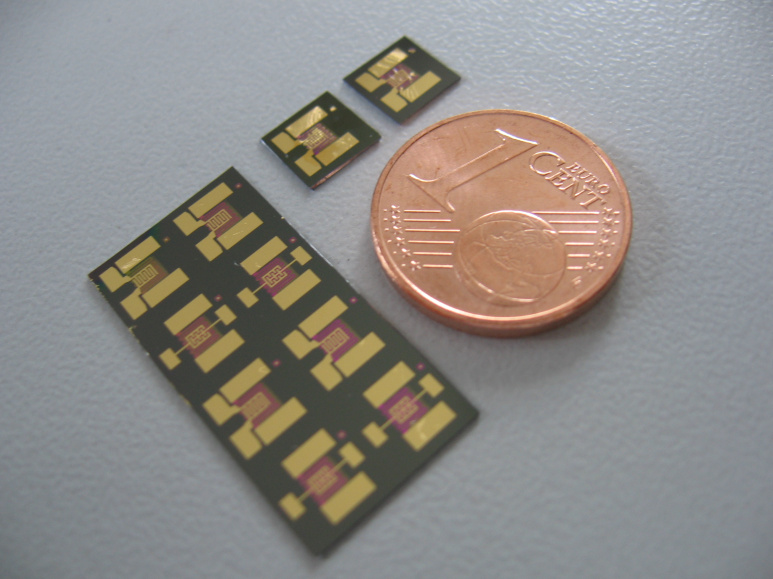
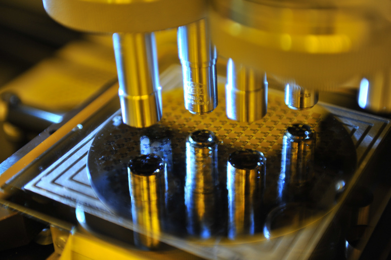
- Micromachining Processing, including photolithographic transfer of device layouts (also available in double-side mode), etching tests of electronic/MEMS materials by wet and dry processes, deposition of metal, dielectric and alloy thin/thick films by CVD, PVD and electroplating, deposition/transfer of 2D materials (graphene) on devices, thermal treatment of materials/devices in high temperature ovens and RTA treatments. Contact person: Matteo Cocuzza (matteo.cocuzza@infm.polito.it).
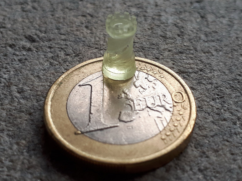
- Polymeric Machining & Additive Manufacturing by processing of elastomeric and thermoplastic materials by hot-embossing, casting in-situ and electrospinning and creation of models for packaging and other applications using 3D polymer printing. Contact person: Luciano Scaltrito, luciano.scaltrito@polito.it.
- Characterizations of electronic “special” devices and materials, mainly characterization of solar cells under AM1 - AM1.5 conditions and tests and characterizations of piezoelectric materials. Contact person: Andrea Lamberti (andrea.lamberti@polito.it).
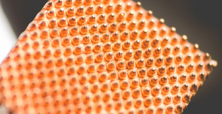
- Laser micromachining by means of Laser Direct Patterning (LDP) (micro-structuring on the surface creating special pattern and/or surface modification) , micro drilling (holes and slits in micrometric useful in wire shaping, micromechanical devices, microfluidics and optical applications), cutting (high precision machining ), engraving, graphitization, ... on different materials such as metal (Copper, aluminum, steel, brass, etc.), ceramics, glass and polymers (Ex. PC, PE, PMMA, PP) and devices. Contact person: Luciano Scaltrito, (luciano.scaltrito@polito.it).